How to make a simple PCB
In this chapter the making of a simple PCB will be described.
The making of the PCB will be divided into a number of steps.
Create a new project
Create a new project:
Action
- Use the menu item
New designfrom the design managerFile menuto create a new project.
In the next dialogbox (window) some parameters must be entered.
Action
- Fill in the first editbox (Design directory) your new project directory. For example
c:\pcb_elegance\simple. - Fill in the second editbox (Design name) the name of your project. This name can be the same name as the project directory. In this case
simple. - Fill in the third editbox (Top sheet name) the name of the schematic of this project. This name can be the same name as the project directory. In this case
simple.
After clicking OK the new project will be created. In the directory c:\pcb_elegance\simple a number of files and directories will be created.
After creation of the project the schematic must be drawn.
Action
- Click on the button
Schematic.
After clicking this button the Schematic editor will be started with the schematic simple.sch. Inside this schematic we will import some symbols, and connect them with wires.
In this simple example we will use the following symbols/components:
- 74HCT14
- Resistor
- Capacitor
- Capacitor (Electrolytic)
- Two pins header
- Power terminal
- GND
- VCC
There are two methods to import symbols/components:
The first and direct method will import a component. A component is a symbol with all the required parameters (The required parameters are reference name, value name and the geometry).
The second method is to import symbols. After importing such a symbol, the value name and the geometry are empty and must be filled in later.
To demonstrate the two methods we import the TTL device, resistor, capacitor and the two pins header via the first method, and import the capacitor (Electrolytic), power terminal, GND and VCC via the second method.
Import the TTL symbol/component 74HCT14:
Action
- Open the right mouse button menu by clicking on the right mouse button. A menu will be visible. Now select menu item.
Add database component->IC->7400 series->74HCTxx.- In the next dialogbox (window) select the item 74HCT14.
- After clicking on
OKthe symbol can be placed.
The other symbols (resistor 10k, capacitor 100n and the two pins header) can be added similar.
Resistor 10k:
Action
Add database component->Resistor->Through hole->Pitch 5- Select 10k
Capacitor 100n:
Action
Add database component->Capacitor->Through hole->Pitch 5- Select 100n
Two pins header:
Action
Add database component->Passive->Connectors->Headers- Select Header2
Importing symbols by using the second method.
Action
- Open the right mouse button by clicking on the right mouse button. A menu will be visible. Now select menu item
Add symbol. In the next dialogbox (window) select the itemC:\pcb_elegance\symin the top listbox.
All the symbols available in the directory C:\pcb_elegance\sym will be listed in the bottom listbox.
Action
- Select the symbol ELCO (capacitor electrolytic). This symbol can now be placed.
- Import the symbols GND,VCC,Power terminals (CON1) similar.
After placing the symbols, some parameters must be edited.
Action
- Select the ELCO symbol. Open the right mouse button by clicking on the right mouse button. A menu will be visible. Now select menu item
Edit text. - In the next dialogbox (window) edit the value and geometry field. Fill the value with 10u, and to fill in the geometry field, click on
select geometrybutton. There will be another dialogbox visible with all available geometries. Now select the geometryelco1_rad6mm. A new window will popup which show this geometry. Click on theOKbutton and the geometry will be placed into the geometry field. Click on theOKbutton and the symbol parameters will be activated. - Modify the parameters of the two power terminals similar, and use the geometry
point_1_1.
The GND,VCC symbol do not need a geometry. After placing those symbols on the sheet, wires needs to be drawn to connect the symbols.
Action
- Click on the wire button or press the key
wto start a wire. - Draw the wires as shown in the figure below.
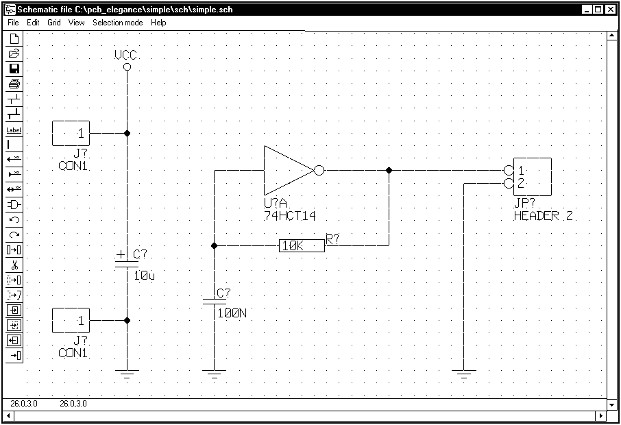
Action
- The schematic is now ready, and can be saved by clicking on the save button.
- Exit the schematic drawing.
Annotate schematic
The schematic needs to be annotated.
Action
- Click on the
Annotatebutton in the design manager, and - Click on the
Restart annotationbutton. Now click theOKbutton in the messagebox.
The schematic will now be annotated. Before annotation the reference
of the resistor was R?, and after annotation R100.
Create netlist
The schematic is now ready, and the netlist should be made.
Action
- Click on the
Netlistbutton in the design manager.
Create layout
The netlist will be created, and will be used by layout editor.
Action
- Click on the
Layoutbutton in the design manager.
The layout editor will be started. In the next dialogbox (window) the parameters of the new PCB should be filled in.
Change the following parameters:
Action
| PCB size | Width | 100 mm |
| Height | 100 mm | |
| Design rules | Trace width | 0.2 mm |
| Clearance | 0.2 mm | |
| Silkscreen | 0.2 mm | |
| Via definition | Pad size | 1.0 mm |
| Drill diameter | 0.4 mm | |
| Clearance | 0.2 mm | |
| Solder mask | 0 mm |
Action
- Click on the
OKbutton, and the PCB will be made visible.
Import netlist
After creating the PCB the netlist must be imported.
Action
- Use the menu item
Import components/netlistfrom theFilemenu and choosesimple.netin the open window to import the netlist.
Place components
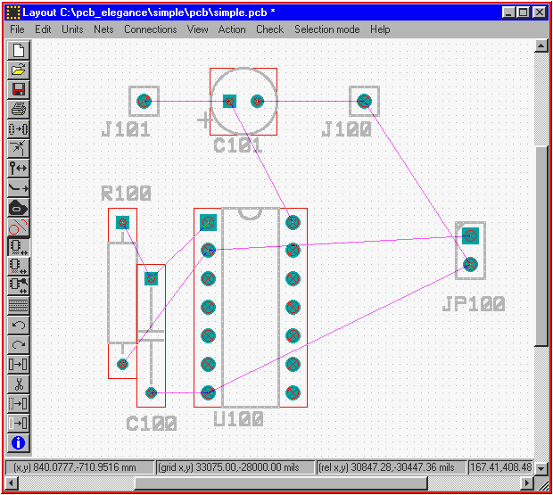
After importing the netlist a number of components should be placed around the PCB. The components should be moved inside the PCB.
Action
- Select the component to be moved. To select a component place the mouse on a component and press the left mouse button. The component will be selected (White) and by pressing the key m or right mouse buttons menu item
Movethe component can be moved. When moving is active, and the right mouse button is pressed the component will rotate.
The green wires indicates which pins should be connected to each other.
Action
- Move the components as shown in the figure below.
Route traces
After the components have been placed, traces must be routed (drawn). Before traces can be drawn the Trace menu should activated.
Action
- The Trace menu can be activated by using the right mouse button menu (
Other menus->Routing menu), or by pressing the keys.
To start drawing a trace, click on a pad or green wire. When trace drawing is active, the current net pins will be marked. To end a trace place the mouse cursor in the neighborhood of a pin, and the trace will snap to that endpoint.
During trace drawing switching to the other can be done by using the right mouse button menu Select layer -> Choose layer.
Check PCB
After all traces have been drawn (No green lines visible anymore) the design must be checked for (design rule) errors, and connectivity errors.
Action
- Use the menu item
Connectivityfrom theCheckmenu to check the connectivity. If there are no connectivity errors a messagebox will be shown. - Use the menu item
Design rule->All layersfrom theCheckmenu to check the design rules. If there are no design rule errors a messagebox will be shown.
The PCB is now ready and should be saved, by clicking on the save button.
Create output files
After finishing the PCB the output files should generated. There are three output options:
- Gerber output plots
- Penplot output
- Output to a printer
Generate gerber output plots:
Action
- Use the menu item
Output gerber/drillfrom theFilemenu to generate the gerber output plots. In the next dialogbox the layers can be selected, the gerber output format (RS274D or RS274X), X mirroring, plotting board outline and the gerber output number format can be selected. There are also two editboxes available. In those two editboxes (each four lines) some information about the PCB can be stored. This information will then be plotted additionally for each layer. After clicking theOKbutton the gerber files and drill file will be generated.
Generate penplot output:
Action
- Use the menu item
Output penplotfrom theFilemenu to generate the penplot output. In the next dialogbox the layers, scale factor, pensize(s), origin, plotting board outline and mirror X can be selected. After pressing theOKbutton the plotfiles will be plotted to the files penplot.*. If possible drill holes will be left open, by shorten traces. After clicking theOKbutton the penplot files will be generated.
Output to a printer
Action
- Use the menu item
Output penplotfrom theFilemenu to generate the penplot output. In the next dialogbox the layers, scale factor, drawing board outline and mirror X can be selected. After clicking theOKbutton the plotfiles will be printed. (All the drill holes will be open)